
It has been a long road. I have started video scaling project since 2023 and have learned the very hard way what is possible and not possible. I conceptually have a type of framework in mind to complete this project. Initially, I got the PSP-1000 slightly working with a levelshifting card and Tang Mega 138K development board by sipeed in 2024. Last year I actually was able to get 720P video working with PSP but I had signal reflection/integrity issues. The DDR3 controller by Gowin operates by a large clock and the DDR3 controller clock itself is the DDR3 clock output divided by 4. So operating at 720P, the systemclk is 74.25mhz and ddr3 clk is 297mhz.
I did try forcing the DDR3 to run at 594 Mhz. The PLL failed to lock so I couldn’t get 1080P out of it. The heatsink also got really hot.
So the new design I have leaned on is using:
-RP2350 MCU. The firmware is capable of updating the FPGA firmware via openfpgaloader and it also configures the HDMI transmitter. I have slowly as a hobby worked on this on and off. I ported vendor i2c firmware and also the dirtypicojtag project to RP2350A. This has been complete for over 6 months at this point. Ready to drop in.
-GW5A FPGA from Gowin. Very specifically the GW5A-EV25PG256CC1/I0 which is a 22nm part with roughly 23K logic elements. As of writing now, the test firmware that calibrates SDRAM and forces two video pipelines to have a test pattern is roughly ~2500 logic.

So we have a lot of headway to say the least. I don’t even think video scaling pipeline will take up a quarter of the logic and BRAM available. I also switched to SDRAM because I shouldn’t require heatsink or fan for it hopefully.
That was an issue if DDR3 was even choosen since that will need heatsink + SDRAM for stability. Even with that…I was getting lock failing. So 16 bit wide SDRAM it is.
Finally, I choose a MIPI to HDMI transmitter. MIPI for those that are unaware is a video interface for mobile systems typically used in tablets or phones. iPhone or Droid phone likely uses MIPI for it’s display. It carries the same types of data as HDMI video except it’s in a byte packet type format instead of a data-island type format like HDMI.
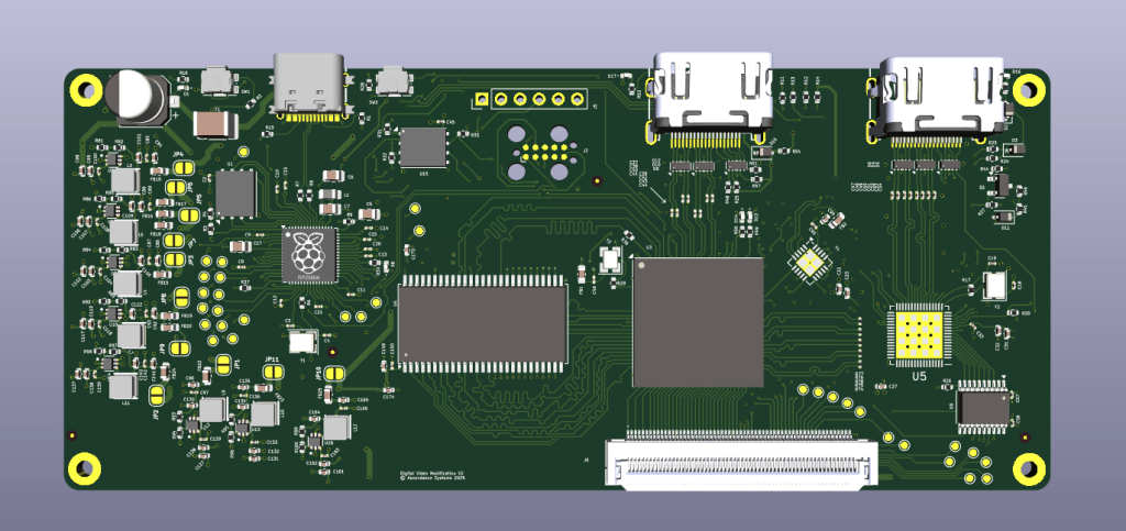
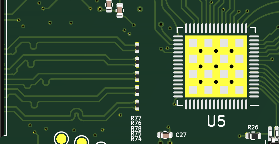
U5 is our HDMI transmitter that isn’t fully wired. This is version 2 of the board. Version 1 had improper footprint. An expensive mistake on my part.
So the USB-C is connected to the MCU. We have basically a ‘reset’ and ‘update’ button for the MCU. So if the firmware for MCU side required an update, we can update it.
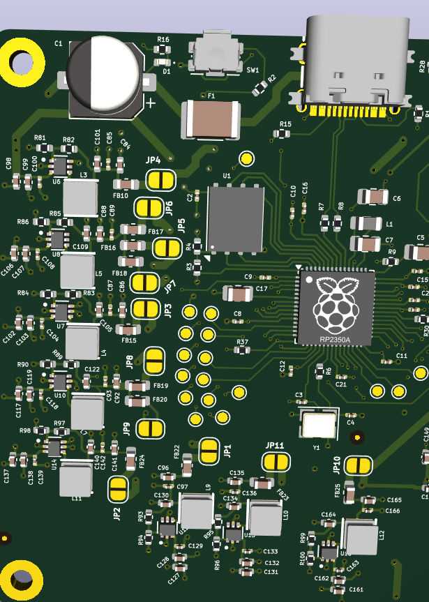
Zooming in we can see F1. It’s a resettable fuse I promise. It’s just that the footprint used was the 0801 capacitor.
We see tons of little buck circuits and the idea was to attempt power sequencing and also splitting the power load so these chips don’t get hot. The goal is to ultimately place this in an enclosure with no air circulation. I also added non-connected jumpers so I can monitor the voltage BEFORE I send it into the rails. This is more of something precautionary so I can verify and measure each voltage before sending it down a rail. I don’t want to pop or crack my FPGA.
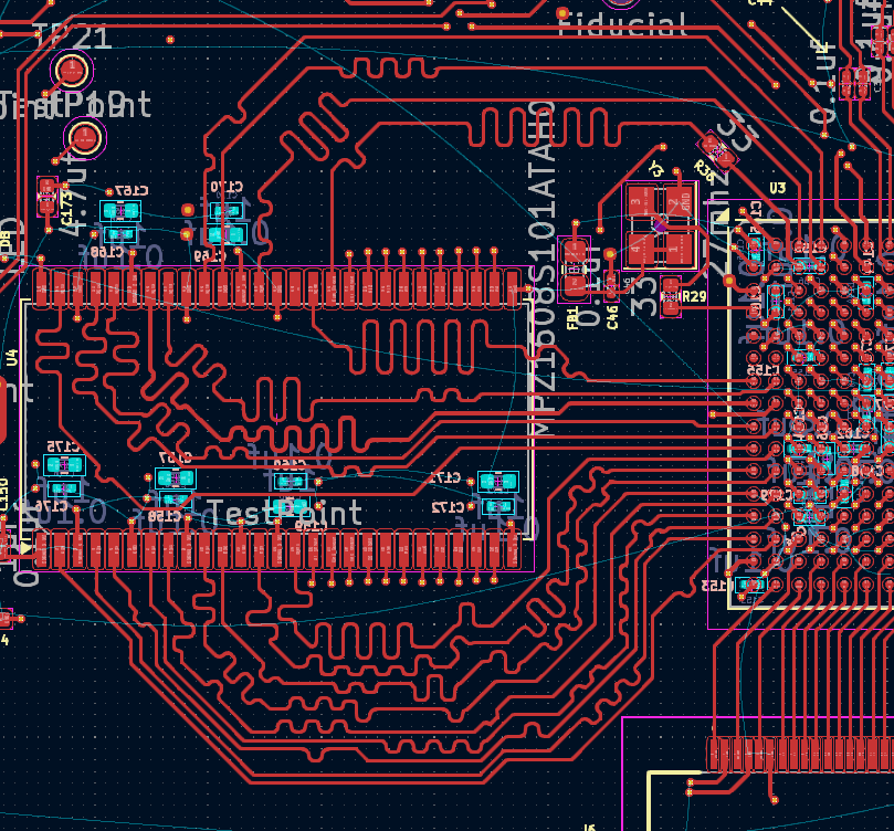
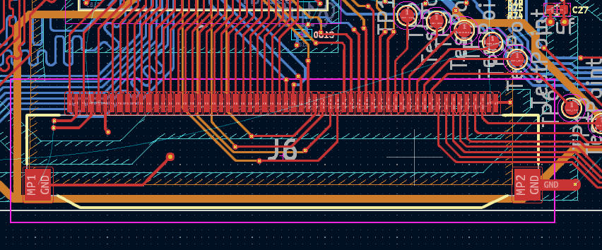
The SDRAM traces on the top and bottom look squished or squiggly because….we will run it at our outgoing pixel clock speed. Yep. We are doing it. So the system clock will be the 1080P pixel clock. Trace length matching was done very carefully and each trace should be within 11 mils of each other for precision.
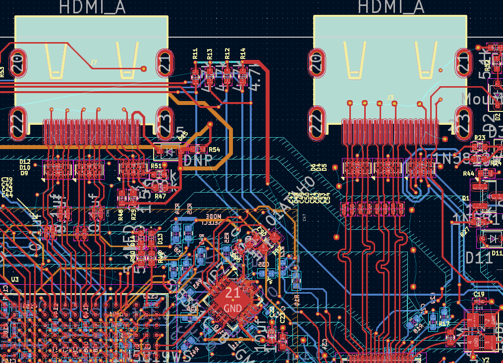
We have two video output regions. The one on the right is 1080P video. The one on the left is more of a bonus output. I had enough pins left to do this and enough bram to implement the HDMI softcore by sameer as a bonus or auxillery output. The plan is for that port to have 1440x240P for GBA, DS (GBA usage only), and NGPC. For PSP, it will be 640×480 just like the component cable. So technically this entire project is 1 video input in, and two out at different resolutions. Firstly, 1080P will be focused on.
I already tested 1440×240 by modifying sameer’s video core with the correct parameters and used a DAC circuit outside of this. It was prototyped and tested on the Tang 138K board first and it was fine. The softcore doesn’t use that many logic elements for it’s pipeline and the serializers should work fine.
If you check the QFN20 chip that is to the right of the FPGA, that is a PLL chip called Si5351. My thought was to use this for the PSP-1000; use the source video pixel clock to generate the video clocks for 1080P. However, according to the datasheet the minimum clock is 10mhz and PSP pclk is 9.00013mhz. So, I may just force it and see what happens. If it works, I can skip the SDRAM altogether and do live video scaling for 1080P, matching the PSP screen refresh rate. However, 640×480 would be still triple frame buffered.
After the FPGA grabs the correct pixels from BRAM, we send our pixel into a pixel to byte converter, then a MIPI DSI TX IP, and then a MIPI TX softphy core.
On the left is the MIPI TX system going to the MIPI RX port of the LT9611. There is a good story about this. I actually made a mistake on V1 board design 🙂
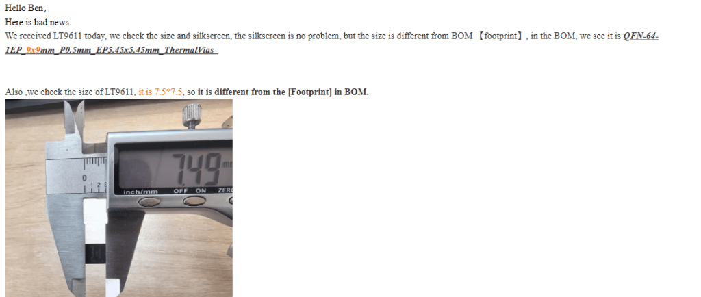
Ouch! They busted the calipers out!

And they superimposed the chip over the board I already had paid for. Sucks and an expensive mistake!
There are also a few other important Gowin-specific things to point out. The part I’m using is a GW5A chip. When selecting MIPI I/O mode for GPIO pins, the IDE does not allow you to select a lower voltage than 1.8V for the bank.
However, Gowin documentation says it should be 1.2V for the….Littlebee (GW1N) 4K and 9K chips?
I had to email Gowin to confirm on the GW5A family of parts, 1.8V must be used to achieve proper voltage swing specification for MIPI DSI.
The only thing remaining is if I need termination resistors or not. The MIPI RX port of the LT9611 is terminated at 100 ohm already. So uncertain if I still gotta do it or not. Again, some Gowin documentation says on the 4K and 9K chips it is required. So it is confusing.
The final significant thing to mention is I placed a 24 pin RGBHV bus on this large FFC connector. The bank is 3.3V so PSP must be level shifted upward from 2.5 to 3.3V. Otherwise, DS, NGPC and GBA handhelds can be directly connected. The idea or concept is to use an interface card to translate any controller signals and video bus signals into that FFC. I already have one complete for the NGPC ready to roll. Just waiting on this card to arrive, perform testing and diagnostics and complete the video scaling firmware.
Upon getting the word from Gowin about those termination resistors, I will start V2 fabrication and get it within ~3 weeks.

Leave a comment