
The Nintendo DS is a handheld I never had growing up. My progress on handhelds was Gameboy Pocket, Gameboy Color and then PSP. So I skipped DS and GBA entirely. Might make sense as to what I play on emulators and FPGA consoles now.
The DS is unique in that it has two screens and in addition to that, a touch screen. Now the touch screen is it’s own problem and for this post, I won’t be touching that yet.
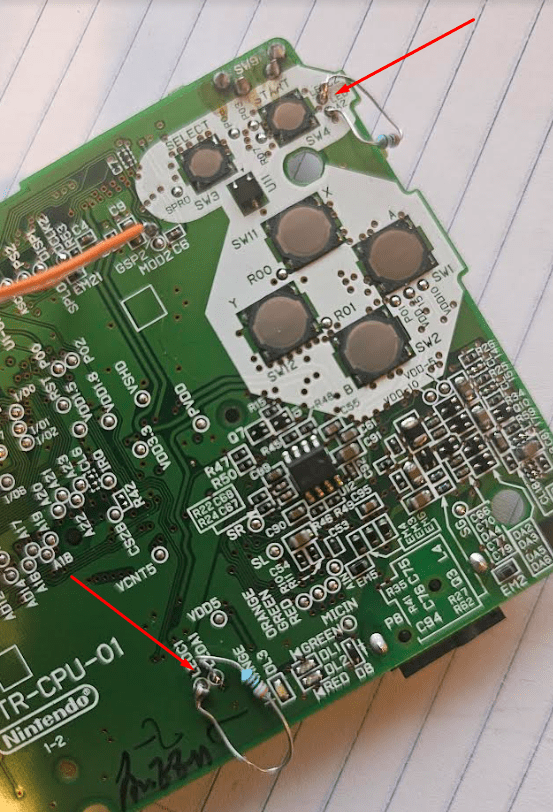
The common DS Macro or GBA Macro mods show bridging the LED A2 and LED C2 points with a 330ohm resistor. This tricks the DS to booting without the top screen. The same can happen when bridging a resistor to LEDA1 and LEDC1. The DS can fully boot without screens attached doing this to the mainboard.
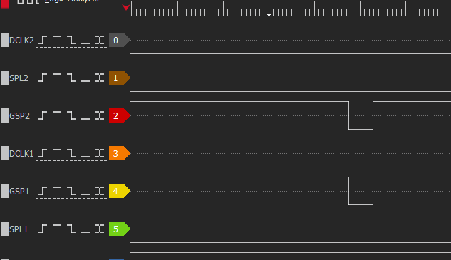
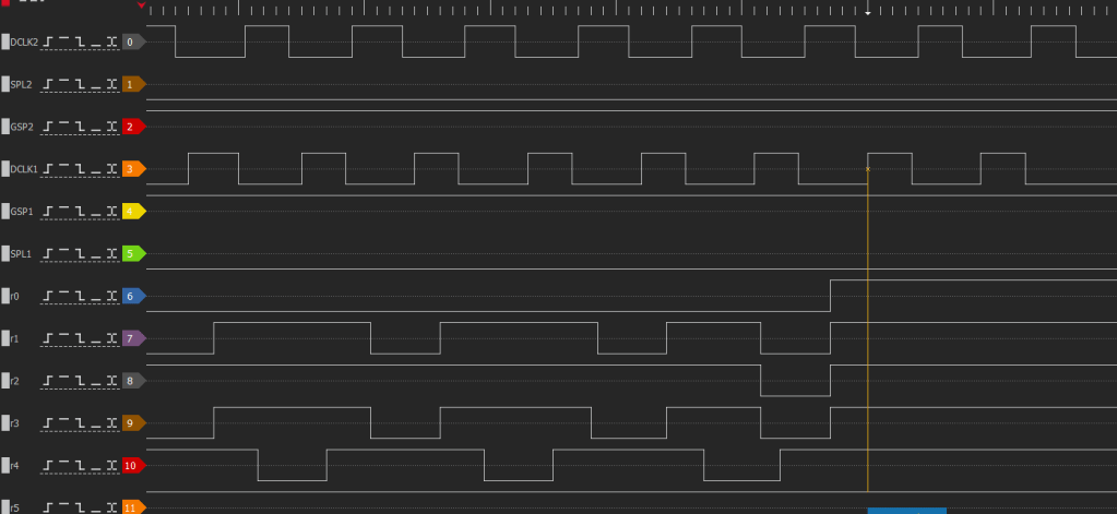
The DS has two Pixel Clocks, Two HSYNC and two VSYNC lines for each screen that it uses. I first tried to use commercial off the shelf FFC connectors to plug into the DS and then put in a breakout cable.
Nintendo labeled the Pixel clock as DCLK1, DCLK2. The Vsync is GSP1, GSP2. The Hsync is SPL1, SPL2. All of these testpoints are visible on the mainboard. What is funny is Nintendo has the same exact color pins going to both connectors. Literally the same pins on the CPU branch out in two directions on the board. The DS homebrew wiki has this mapped out as well. Hardmod | DS-Homebrew Wiki
The next step is to actually capture the behavior of the DS screen. At first I thought putting a flex cable with a breakout board as appropriate.
There is a problem with this approach when I noticed sometimes the DS wouldn’t turn on, pins were randomly grounded and I couldn’t get any reads. The problem was visible once I lined up the flex cables.
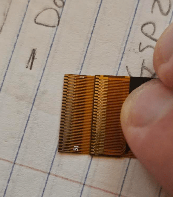
The cable on the left is the one I sourced and the one on the right is from one of the screens. It’s ever slightly wider and the FFC connector is built to accommodate this. So you can’t reliably center the FFC at all.
So unfortunately that was a waste of time. It looks like for any reliable approach in consolizing the Nintendo DS, a flex PCB will be required for specifically the video. You can actually only grab the video data for both screens on shared points. I will explain why this is now.
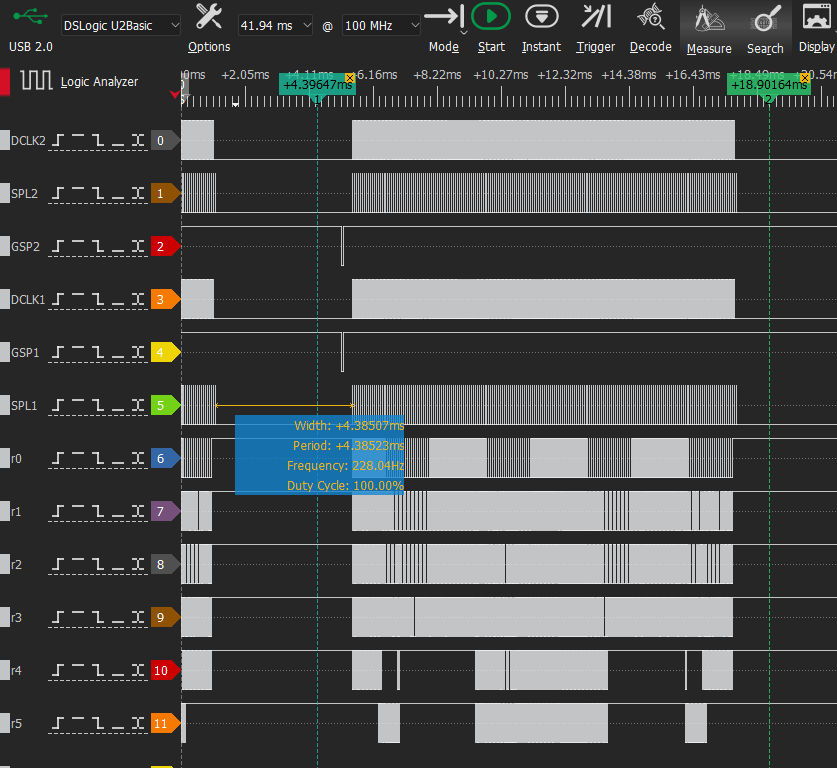
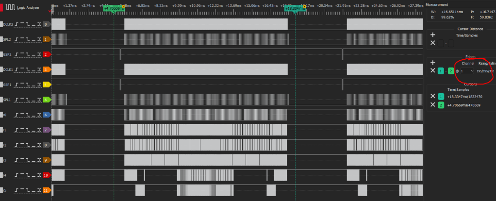
The photo above shows 1 video frame going on both screens at once. There is something really important to point out from this capture.
As DCLK2 rise, DCLK1 fall and the colors change. Again, similar to DDR.
New video frames start at the same exact time! So that makes things easy.
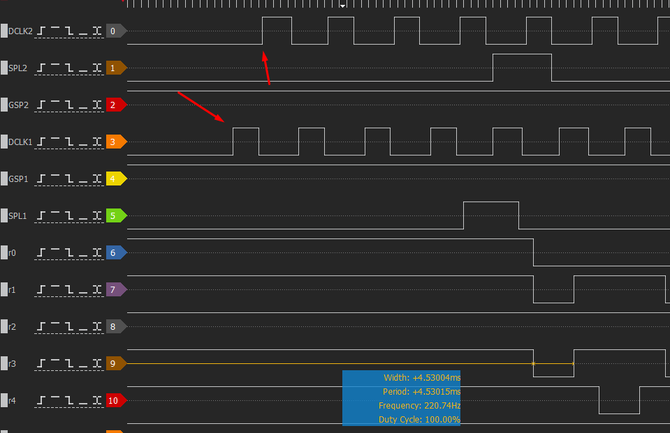
Now as DCLK1 goes high, the bottom screen is latched. As DCLK1 goes low, DCLK2 goes high. Then the top screen is latched. With this interpretation, you can process the data as DDR.
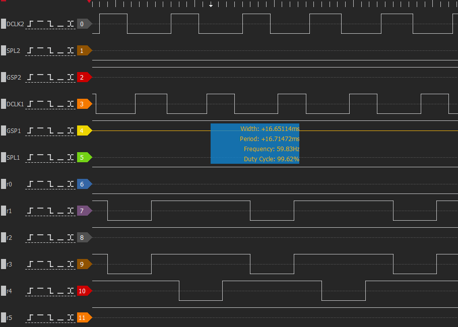
Now the DS screen resolution was 256×192. The pixel clock however pulses more than this.
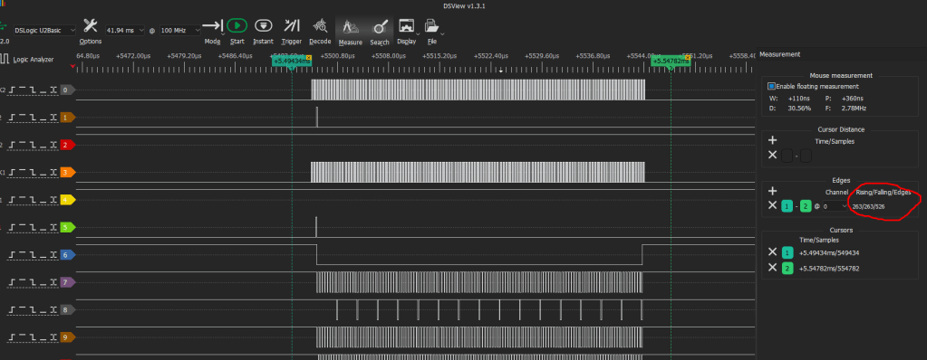
It pulses approx 263 times per line. So 263-256 = 7
So we have 7 extra pulses we need to account for and ignore. Well, pay attention to but during those 7 pulses, ignore processing incoming pixels into the FPGA.
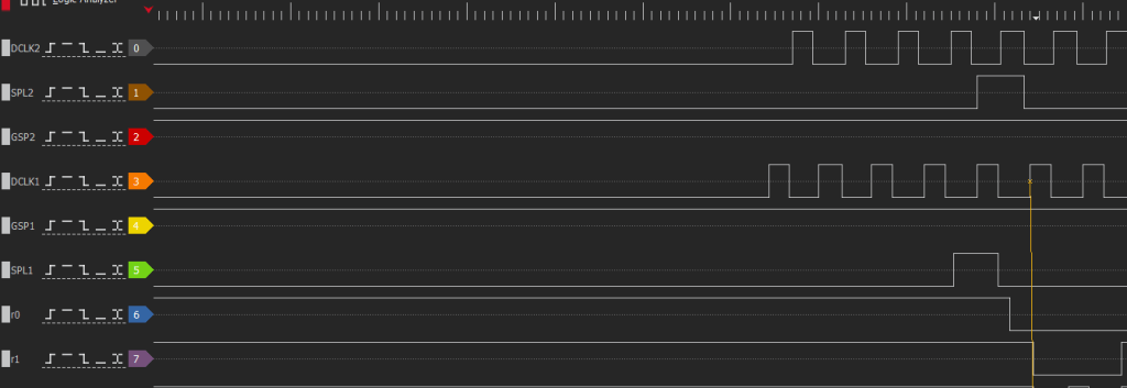
5 Pixels before the line starts. Line starts at SPL1/2. You could clock it on a single SPL line technically.
The last 2 pulses are at the end of the frame. So the extra pixel clock pulses are now accounted for.
Now we have to see if there is any extra line pulses.
And there are. 195-192 = 3. We have to find 3 extra line pulses.
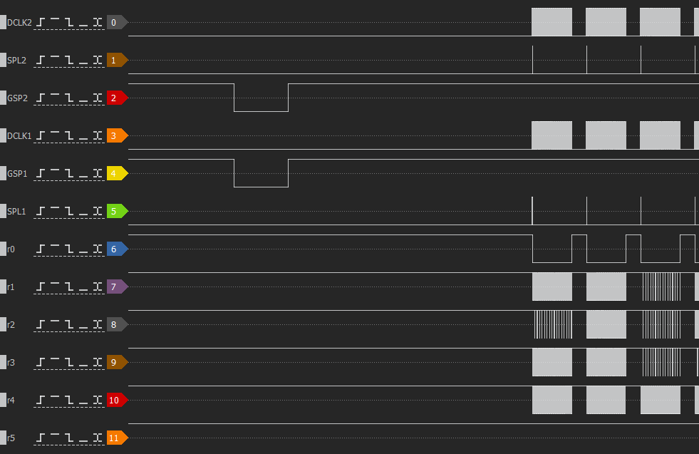
They’re not in the front.
They’re in the back!
So now that all of these are accounted for, it is possible to build a state machine that writes pixels to BRAM in the FPGA and then further to a frame buffer.
Actually, I should now explain what direction I will go with this. My first thoughts are to make a GBA consolizer with the DS and eventually DS Lite. These can run GBA carts fine with the bottom screen. So only the bottom screen pixels would have to be read which is trivial to scale. Actually, the framework for the NGPC can be modified easily to accomodate this pattern.
A Super Nintendo controller can run all the GBA style controls totally fine on a DS if it’s just running GBA games. The reason this is an attractive method to play GBA games on TV is that a broken DS is MUCH cheaper than GBA. The handheld modders really ate up all the broken or junk GBAs for sale to the point where prices are pretty nuts.
Meanwhile I bought a lot of 11 junk DS and DS Lite for $70 USD from Japan before shipping. I think it’s just a more economical way to get video out.
So any first digital video modification for the DS would be more of a GBA consolizer. An actual DS consolizer in my eyes will require the following:
-Framebuffer due to how the screens are drawn. There will be 1 line of latency.
-Touch screen emulation. Removal of touch IC is required, and manipulating the PENIRQ and SPI lines directly to the CPU will be required.
–Video mixing of a touch screen emulation “pointer” on the screen.
–90* screen rotation mode. This is probably the hardest thing to do. Touch screen pointer must also change position when rotated.
Those two are pretty tall orders but possible given enough time, it can be done.
Also, there may be some readers wondering why I never mentioned the DS Lite. The DS Lite will require a slightly different approach due to the fact that the color pins and video control pins are seperate and not branched off/shared. I have an idea of how to tackle it, I don’t like it, but there is a way.
Shifting to audio, I tried to find anything that resembled an i2s audio source on the mainboard. There isn’t one even hours of poking around the Mitsumi ASIC that handles power and digital to analog conversion.
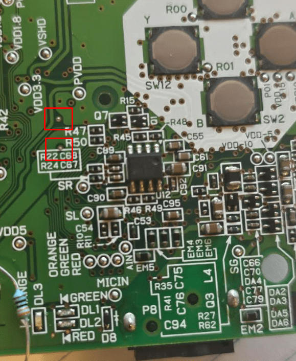
However these points are the digital audio source and they’re PWM. I guess Nintendo decided to recycle that until the DSi.
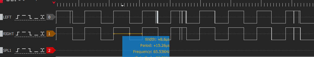
Yep. PWM audio just as suspected. So some PWM to PCM DSP will be required. Then that can be shoved into an i2s transmitter module.
So with all of this information, it’s possible to consolize for GBA games rather easily. The frame buffering and touch emulation for a DS type consolizer will take a substantial amount of time.

Leave a comment