
I’ve noticed in the retro space that there is a common theme to get a handheld and “consolize” it with digital video so it can be played on big-screen TVs. You see really cool projects such as the swancolorHD, GGHD by Gamebox Systems, GBA Consolizer by Woozle, and many other projects.
I noticed the Neo Geo Pocket Color didn’t have a digital video modification yet and sought to attempt to deliver this to the community. At first I thought of doing just a component video. Here is why that may be a bit impractical:
- The resolution of the screen is approximately 160×152 pixels. This isn’t a standard resolution at all.
- Storing entire lines into memory and converting the colors could be off since the depth is only 4 bits per color even with a potentially correct formula. People might not like the image they see although I have no experience performing multiplication in digital design.
- Scaling the 160×152 into proper and sane video format such as standard 640×480
So I decided that it would be impractical for a component video modification because of those factors. Not to mention that modern televisions are beginning to omit composite video inputs and potentially component inputs would be next on the chopping block.
So let’s go over the specifics about NGPC. The colors are output at a depth of 4 bits per color. The Gameboy Advance on the other hand was 5 bits of color depth. So color selection is a bit more limited by comparison. The NGPC has an SoC called the K2 as the primary CPU which does cartridge reading, analog sound output, and digital RGB output which goes into an LCD. Here is a stock image of the board.
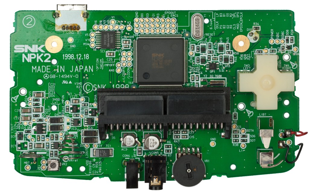
What is nice about this design is SNK labeled many test points on the front AND back side. I don’t think the K2 has a digital audio BUS at all, unfortunately. It has one speaker but does output left and right sound. So stereo sound is present and only accessible on the audio jack.
Here is the following pinout of the LCD for the 36-pin one I have.
P1 (high voltage for lcd)
P2 (negative voltage for lcd)
P3 MOD
P4 SPS
P5 CLS
P6 unknown (all low)
P7 extremely fast clock needs investigating?
P8 extremely fast clock needs investigating?
P9 extremely fast clock needs investigating?
P10 extremely fast clock needs investigating?
P11 SPL
P12 R0
P13 R1
P14 R2
P15 R3
P16 G0
P17 G1
P18 G2
P19 G3
P20 B0
P21 B1
P22 B2
P23 B3
P24 (high voltage for lcd)
P25 GND
P26 PS (need research)
P27 LP 9.17074KHZ
P28 DCLK 1.60123MHZ
P29 (high voltage for lcd)
P30 V0
P31 V2
P32 V4
P33 V6
P34 V8
P35 V9
P36 GND
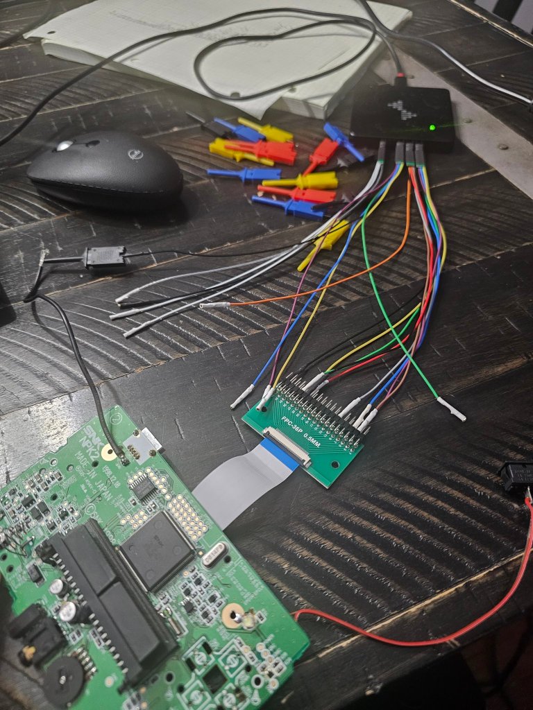
Here are the signals that are significant to us: R0 to R3, B0 to B3, G0 to G3, DCLK, SPS and SPL. The reason I know SPS is the vertical and SPL is the horizontal was due to the activity on the NGPC screen when I would ground those lines. The DCLK is what we would know as a pixel clock. The SPS also has a negative sync polarity which is visible on this capture here. I’ve concluded there is no DE or “data enable” signal for this CPU + LCD combo.
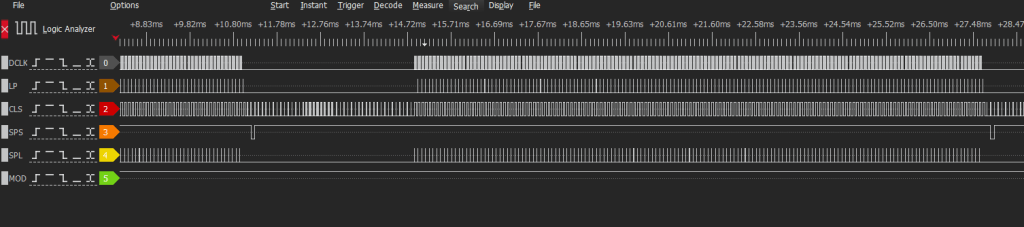
Notice once SPS goes low, it starts a new video frame.
The DCLK runs at a frequency of approximately 1.60123MHZ, the SPS (Vertical) at 59.9546HZ and the SPL (Horizontal) at 9.17074 KHZ. With these frequencies and timings in mind, it should be possible to construct a design inside an FPGA to grab these screen values and perform line and pixel multiplication to output a 1080p digital video image. However, the crutch to do this first is on a known devboard before spinning new hardware. The design pipeline is to first accomplish 640×480 VGA video. Once that is verified to work, the digital video stream can be sent to an HDMI serializer/transmitter provided it’s configured on the i2c.
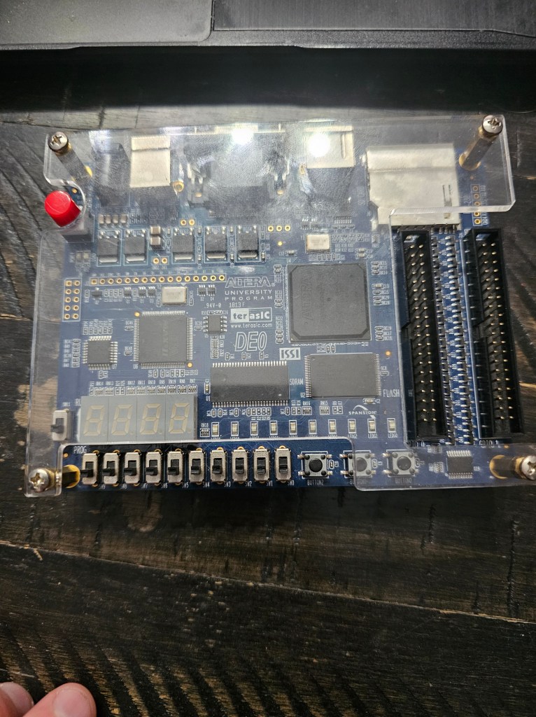
The DE0 by Terasic contains a Cyclone III with 15K LEs, tons of GPIO on the right side, and most notably a 4-bit resistor DAC VGA network. So 4 wires per color as the video already is from the NGPC. Once the design is verified on this board at 640×480, I can port this over to an FPGA by Efinix. Currently, the 50mhz clock signal can’t hit the 148.5Mhz pixel clock required for a 1080p video framework but I think with cascading PLL it could be achieved.
It should be noted the NGPC video is 3V logic but the GPIOs are configured for 3.3V logic according to the schematic indicated voltage for the voltage banks. I think it will be enough to get away with. If not I will need to use level shifters.
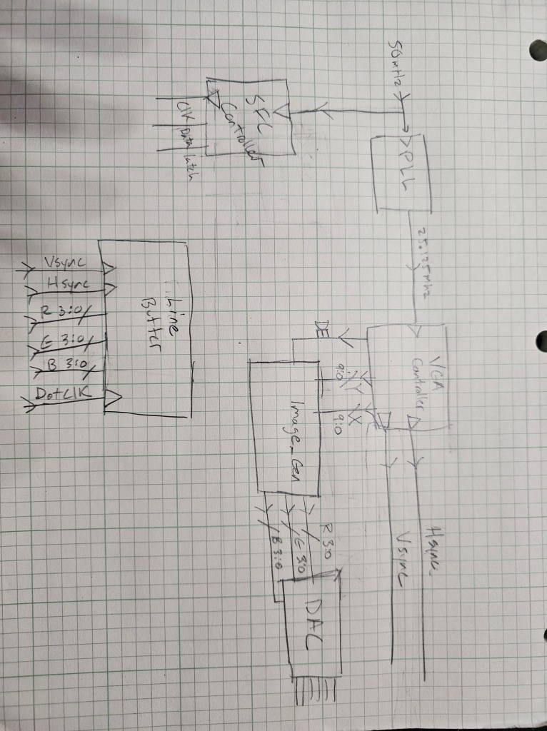
Here is a very hazardly high-level design of the pipeline that I’ll be designing. SFC Controller, NG Controller logic, VGA controller and Line buffer all work. The image generator along with pixel and line multiplication will be the biggest challenge. There should be borderline zero latency with this approach as it will draw and multiply as the screen data comes out of the NGPC.

Leave a comment